Jumat, 10 Juli 2009

Sapphire Radeon HD 4670 512MB GDDR4 Video Card Review

Author : Austin Hamann -

Published : Tue, Jul 07, 2009

The Budget Minded Sapphire Radeon HD 4670

Sapphire HD4670 512MB

The Sapphire HD4670 512MB


The video card market is an ever-expanding one that sees new cards from ATI and NVIDIA alike month after month. Granted, some are just core refreshes or 're-branding,' but there is always something new. Usually cards that are released in between series updates offer a good price/performance ratio, and lower the price of main cards as well; two of those cards will be compared today. Up on the review block are the ASUS GeForce 9600 GSO 384MB and the Sapphire Radeon HD 4670 512MB.


Specifications

ATI came out with the 4600 series cards some time ago; these are basically the mid-range offering, lower than the 4770 and 4800 series but above the 4300 and 4500 series. With so many new cards out there, this 4670 fits in nicely to the sub $70 market, which seems to be offering better and better performance every month. The Sapphire Radeon HD 4670 that we are looking at today can be purchased online for $69.99 shipped, for example.

Both Cards

Looking at the pictures of the cards we will be reviewing, the GeForce 9600 GSO seems a lot burlier. Though both of the cards' fans are effectively dual-slot sized, the GeForce 9600 GSO is approximately 2 1/4” longer and requires a 6 pin power connector which the Radeon HD 4670 GPU does not. Let's take a closer look at the Radeon HD 4670 video card and see if it's more powerful than it looks.

Retail Box and Bundle

Retail Box

Looking at the box, you can see some of the big features. It supports 7.1 channel audio (over the HDMI connection), has 512MB GDDR4 VRAM, and has an 'ultra silent' heatsink fan rated for less than 20 dBA, which is just amazing for a video card fan.

Bundle

The bundle that comes with this card is a little slim, but for good reason. It doesn't supply any converters due to the variety of onboard connectors already there and it does not have the usual molex-PCIe power connector as again, none is needed since it takes its power from the PCIe slot alone. The user manual is pretty standard: how to install the card after removing an existing one, a small section for troubleshooting, and everything offered in 7 languages. The only thing that the manual, and any user manual I've seen, is missing is the driver installation and driver updating, as this is what many end-users get hung up on after all. Of the discs provided, there is the driver disc (of course) for those who want drivers they know will work. Catalyst 8.10 is what came on this disc. Another is Ruby ROM which holds three game demo's (Call of Juarez, Dungeon Runners, and John Woo Presents: Stranglehold), several high resolution wallpapers for ATI graphics (oddly, advertising the HD2000 series) and AMD Processors among others, a screensaver, and a couple of other apps. Also included in the bundle are Cyberlink's PowerDVD and DVD Suite for those who use the card as an htpc -- these discs will come in very handy. Also included in the bundle are the trademark 'Powered by Sapphire' sticker and Crossfire bridge.

A Closer Look

Closeup

Measuring in at 6.56” the Sapphire Radeon HD 4670 video card features 512MB of GDDR4 VRAM at 1100MHz (2200MHz effective), a 128 Bit Bus width, 750MHz on the core clock, 514M transistors and 320 Stream Processors. On paper this little thing packs some punch, and with two Crossfire interconnects, you can get a solid CrossfireX system on the cheap.


Back Side of the Card

The back of the card is fairly unique in that it uses individual IC heatsinks on all the memory ICs, which is not particularly common even on most higher end cards. But anything that looks cool, doesn't get in the way, and helps with heat is fine by me.


Connectors

This card offers nice variety in its display connectors, with Dual Link DVI, VGA, as well as HDMI out, so no converters are necessary for the majority of applications.


Crossfire Interconnects

ATI has taken it upon themselves to design nearly every PCIe full-width card with two crossfire connectors for CrossfireX, whether providing two interconnects is better than one has yet to be seen, as most end-users in this price range aren't considering more than two, if that. If it isn't costing them much more money to throw that second interconnect on, why not?


Core

With the heatsink and fan off we see the 55nm RV730XT core which produces a nice 480 GFLOPS of processing power; not bad for a card that retails for as low as $69.99.


GPU-z

Using GPU-Z 0.3.4, we can see all the little details about this card: from BIOS version to Driver version, to Pixel and Texture Fillrates and more. There is nothing special here so we'll move on to the test system.

The Test System

The Test System

The test system was running XP Professional with Service Pack 3 and all available Microsoft updates. The Sapphire 4670 was using ATI Catalyst 9.3 drivers due to artifacting on new drivers, and the ASUS 9600 GSO was using nVidia Geforce 181.20 Cuda Drivers for the same reason. All results shown in the charts are averages of at least three runs from each game or application used.


The Video Cards

  • Sapphire Radeon HD 4670 – 512MB GDDR4 (750MHz/2200MHz)
  • ASUS Geforce EN9600 GSO TOP– 384MB GDDR3 (600MHz/1800MHz)

The test system used was a little more modest than the one ordinarily used for video card reviews, featuring an Intel Core 2 Duo E7200 'Wolfdale' clocked at 3.20GHz in an EVGA 750i FTW SLI motherboard with 4GB of system memory. The Corsair XMS2 2x2GB kit was used at stock speeds of 800MHz, and 5-5-5-18 timings. The E7200 was used with a MASSCOOL 8WA741 92mm Ball CPU Cooler. Keeping in line with the rest of the system being 'budget' based, this tower cooler rings in at just $23 and keeps the chip at good temps even at a nice stable 3.2 GHz; this is an underclock compared to normal use, but rock solid. Powering the system is the Corsair TX750W Power Supply with a single 60Amp 12v+ rail.

Test Platform

Component Brand/Model Live Pricing
Processor Intel Core2 Duo E7200
Motherboard EVGA 750i FTW
Click Here
Memory 4GB Corsair DDR2 800MHz
Click Here
Video Card
View Above
Click Here
Hard Drive
Western Digital Raptor
Click Here
Cooling MASSCOOL 8WA741 92mm Ball Click Here
Power Supply
Corsair TX750W
Click Here
Operating System
Windows XP Professional SP3
Click Here
Now that you know the rest of the system used, we can continue on with the testing.

3DMark06

In-Bench Screenshot

3DMark 06 is the worldwide standard in advanced 3D game performance benchmarking in DX9.0. 3DMark06 tests include HDR/SM3.0 graphics tests, advanced SM2.0 graphics tests, AI and physics driven single and multiple cores or processor CPU tests and a collection of comprehensive feature tests to reliably measure gaming performance. Default 3DMark06 settings were used for testing, so a resolution of 1280x1024 was used.


3DMARK Overall Performance Chart SM 2.0 & 3.0 Performance Chart

The overall score is no comparison, with the GSO outscoring the 4670 by over 2000 3DMARKs. The SM 3.0 score is slightly closer with the GSO getting 600 more points, but the SM 2.0 test has over a 1600 point difference between the two, again in the favor of the GSO. So, there is a clear winner in synthetic testing. That is the last of the testing, so now it is on to the final thoughts and conclusion.


Final Thoughts & Conclusion

closeup

The Sapphire Radeon HD 4670 and GeForce 9600 GSO with 96 stream processor that we test today are two great graphics cards that one can find in the $75 price range. To be specific, the Sapphire Radeon HD 4670 can be found for $69.99 plus shipping, while the ASUS GeForce 9600 GSO can be found for $73.99 shipped. At these prices you really can't complain about performance as they did fairly decent in all the games we threw at them.

For temperatures and audible sound from the fan, the Sapphire Radeon HD 4670 wins hands down, with idle temps of 25-30C, it runs about half as hot as the GeForce 9600 GSO which idles at higher than 55C. Additionally, the fan is hardly audible on the Radeon HD 4670 (or at least I couldn't hear it over the sound of my hard drive) unlike the GSO, which has a larger fan that you can hear over all the other fans in the system.

Performance-wise, I'm very impressed with the Radeon HD 4670 because it not only has higher frame-rates in GRiD and L4D, but it never had any issues with choppy game-play in any game. The 9600GSO may have gotten high frame rates in most games, but I can't deny the fact that the HD4670 played better in every game, whether it was running at 15fps or 70, the game play was perfect: no slide-shows, no random errors or crashes. This cannot be said for the 9600GSO, because it periodically got down to 8 fps and game-play would totally stop for up to 20 seconds at the same settings as the HD4670 was on, which ran perfect, never dipping below 45 in any situation. I would not deem the game playable at high settings on the 9600GSO; there is no getting around that. The synthetic test run, 3DMARK '06, showed the opposite performance winner, with the 9600GSO clearly in the lead, no contest, but the average user doesn't buy video cards based off synthetics alone, so take the results of that test with a grain of salt.

All in all, I'd declare Sapphire's Radeon HD 4670 512MB offering the winner as the only aspect that the 96 Stream Processor 9600GSO wins is in the synthetic benchmarking, which isn't the top priority to a majority of users. Though there is one thing that gets on my nerves, which is driver support, now both cards suffer from not being able to use the newest/beta drivers, so this doesn't really affect the comparison of the two as they tie there, it just gets annoying that the user has to hunt down the proper drivers for their card if they want an update from the driver disk version.

Asus Maximus II Gene P45 Motherboard

July 7th, 2009


Asus is one of the leading motherboard makers in the market. As such, they are still cranking out LGA 775 motherboards. Their latest offering sports Intel's popular P45 chipset, two PCIe 2.0 slots, CrossFireX capability, and support for 16GB of DDR2-1300MHz memory. Furthermore, all of these features are available on a microATX form factor that seems ideal for a LAN or HTPC system where size definitely matters. Is this the board you've been looking for? Find out as HardwareLogic throws the Maximus II Gene on the test bench to see if good things really do come in small packages.


With the introduction of Intel's Core i7 platform, enthusiasts faced a tough and expensive decision. As you know, jumping on the Socket 1366 bandwagon consists of a CPU, motherboard, and memory upgrade. The move probably is not appealing to those on a budget and still rocking a decent 775 system. But just because Core i7 is on the scene, Core 2 processor owners still have plenty of options when the upgrade bug bites.

Asus is one of the leading motherboard makers in the market. As such, they are still cranking out LGA 775 motherboards. Their latest offering sports Intel's popular P45 chipset, two PCIe 2.0 slots, CrossFireX capability, and support for 16GB of DDR2-1300MHz memory. Furthermore, all of these features are available on a microATX form factor that seems ideal for a LAN or HTPC system where size definitely matters. Is this the board you've been looking for? Find out as HardwareLogic throws the Maximus II Gene on the test bench to see if good things really do come in small packages.

Product / Model
  • Asus Maximus II Gene
Form Factor / Size
  • microATX / 9.6 x 9.6 inches
CPU Support
  • Socket LGA 775
  • Intel Core 2 Extreme / Core 2 Quad / Core 2 Duo / Pentium Dual-Core / Celeron Dual-Core / Celeron
Chipsets
  • Intel P45 / ICH10R
Memory
  • Four DDR2 memory sockets
  • Dual channel DDR2 1300 / 1200 / 1066 / 800 / 667
  • Up to 16GB maximum capacity
Expansion Slots
  • Two PCI Express 2.0 x16 slots
    - Single max x16
    - Dual x8 speed
  • One PCI Express x1 slot
  • One PCI 2.2 slot
  • Supports ATI CrossFireX Technology
Onboard Audio
  • SupremeFX X-Fi
  • 8-channel High Definition Audio CODEC
    - EAX Advanced HD 4.0
    - X-Fi CMSS 3D
    - X-Fi Crystalizer
    - Creative ALchemy
    - Supports Optical S/PDIF out ports on rear
Onboard LAN
  • Gigabit LAN
USB Ports
  • 12 USB 2.0 Ports (6 rear panel, 6 onboard headers)
Storage / SATA Drives
  • ICH10R Southbridge:
    - Six SATA 3.0 Gb/s ports
    - Intel Matrix Storage Technology supports RAID 0, 1, 5, and 10
  • JMicron 363 controller:
    - One Ultra DMA 133/100/66/33 for up to two PATA devices
    - One SATA 3.0 Gb/s port
    - One External SATA 3.0 Gb/s port (SATA on-the-go)
Onboard 1394
  • Two 1394a ports (one rear panel, one onboard header)
ROG Exclusive Overclocking Features
  • Keyboard - TweakIt Power Design
    - 8-phase CPU power
    - 2-phase DRAM power
    - 2-phase NB power
  • CPU Level Up
  • iROG
  • Extreme Tweaker
  • Loadline Calibration
  • Intelligent overclocking tools:
    - Turbo V
    - OC Profile
  • Overclocking Protection
    - COP EX (Component Overheat Protection - EX)
    - Voltiminder LED
    - Asus CPR (CPU Parameter Recall)
Current Pricing
  • N/A

Bundle

When shopping for motherboards, one of the main features to consider is the bundle. We've noticed that high end boards typically include more accessories than less expensive ones. Let's check out what Asus decided to include with the Maximus II Gene.


ACCESSORIES
  • LCD Poster
  • I/O Shield
  • ASUS Q-Connector Kit (USB, system panel)
  • Cable ties
  • ROG Label
CABLES
  • Four SATA signal cables
  • One Ultra DMA 133/100/66 cable
  • One Floppy disk drive cable
APPLICATION DVD

Asus Motherboard Support DVD

  • Drivers
  • Sound Blaster X-Fi Utility
  • Futuremark 3DMark06 Advanced Edition
  • Kaspersky Anti-Virus
  • Asus TurboV Utility
  • Asus PC Probe II
  • Asus Update
  • Asus AI Suite
DOCUMENTATION
  • ASUS Maximus II Gene Motherboard User's Guide


With higher end boards, we like to take a closer look at the design to see what kind of issues an enthusiast might come across during installation or use of the product. Historically, the Asus motherboards we've reviewed have been impressive in this regard and the Maximus II Gene is not an exception. The color scheme is the same used in other ROG boards we've seen recently, such as the Maximus II Formula and Rampage Extreme. Obviously, Asus decided not to mess with a good thing. In addition, we find the power and data connections along the edge of the motherboard, allowing for easy cable management.

Expansion Slots
(top to bottom)
  • PCIe x16 Slot (Blue)
  • PCIe x1 (White)
  • PCIe x16 Slot (Blue)
  • PCI Slot 2.2 (White)

There are four expansion slots available on this motherboard. Two PCI Express x16/x8 slots are reserved for graphics cards. Each slot provides 4GB/sec bandwidth and supports CrossFire technology. The PCI Express x1 slot houses lower bandwidth intensive cards, such as modem or LAN cards, and provides 250MB/s bandwidth. And the lone PCI slot supports expansion possibilities such as LAN, USB, or SCSI cards.

You'll find four 240-pin DDR3 slots on the board. Each slot supports up to 4GB sticks for a maximum of 16GB of total RAM. Dual channel operation can be achieved by using both blue or white sockets.

Along the edge of the Maximus II Gene are the onboard reset and power buttons. For a board that targets the enthusiasts, having these buttons available is a nice touch. In addition, there are six SATA ports found on this corner of the motherboard. As always, we're very glad to see the ports with the right angle design in order to avoid conflicts with large GPUs.

Rear Panel Connectors
  • PS/2 Keyboard Port (Purple)
  • Six USB 2.0 Ports
  • CMOS Clear Button
  • Optical SPDIF Output
  • 1394a Firewire Port
  • eSATA Port
  • LAN (RJ45) Port
Audio Ports
  • Blue - Line In
  • Green - Line Out / Front Speaker Out
  • Pink - Mic In
  • Orange - Center / Subwoofer
  • Black - Rear Speaker Out
  • Grey - Side Speaker Out


Test System

Processor
  • Intel QX9770 Core 2 Extreme Edition
Motherboard
  • Asus Maximus II Gene
  • Asus P5Q Pro Turbo
Memory
  • OCZ Blade 4GB DDR2-1200
Video / Graphics
  • VisionTek HD4870X2
Hard Drive
  • Western Digital 300GB Velociraptor
Cooling
  • Custom Watercooling
Power Supply
  • Corsair HX1000W
Operating System
  • Microsoft Vista Ultimate SP1 64bit

To evaluate the Maximus II Gene, we used the some of the best components on the market for our test bench. Our QX9770 runs at 3.2GHz stock, 400 FSB with an 8x multiplier, and is watercooled. The 4GB memory kit from OCZ runs at 1200MHz at only 1.8V while the HD4870X2 is still one of the fastest videocards available.

In order to push a motherboard, a dual core processor like the E8400 should be used to find the maximum front side bus speed. Unfortunately, we did not have a Core 2 Duo CPU handy but we still successfully overclocked the QX9700 quad-core to 4.5GHz with watercooling and the Maximus II Gene.


Benchmark

Maximus II Gene
3.20GHz
400x8
P5Q Pro Turbo
3.20GHz
400x8

System


PCMark Vantage
Overall Score
7776 7717

CPU

CPC Benchmark
Image Editing
Video Editing
Multi-Tasking
Overall
1146
1863
1165
1391
1179
1864
1146
1396
Cinebench 10
Single
Multi
3942
14074
3908
14244
Sisoft Sandra 12
Aggregate Arithmetic
48.27 47.47
Everest 4.5
Queen
Photoworxx
22828
25418
22825
25052
WPrime v1.61
32M
1024M
12.027
383.058

12.03
378.844

Memory

1200MHz
5-5-5-15 2T
1200MHz
5-5-5-15 2T
Sisoft Sandra
Aggregate Memory
8.6 8.5
Everest
Read
Write
Copy
Latency
8626
8506
8726
59.9
8243
8503
8686
64.3
Super Pi V1.5
1M
32M
14.508
14.24.333

14.555
14.29.357

Gaming

3DMarkVantage
FarCry2
P14291
14.39
P14280
14.28


Section

Score

Comments

Layout

10/10

  • Excellent design
  • CPU socket and memory areas free of obstructions
  • Right angled SATA ports
Features

10/10

  • Micro-ATX
  • Up to 16GB of DDR2-1300
  • x16 PCIe 2.0 expansions slots (x8 each for dual-cards)
  • CrossFireX Support
  • Onboard Power, Reset and Clear CMOS switches
Bundle

8/10

  • LCD poster, I/O shield, and Q-Connectors
  • Support DVD filled with relevant drivers
BIOS

8/10

  • Easy to navigate
  • Lots of options
Stock Performance

18/20

  • Stable out of the box using Auto settings
  • Chipset heatsinks only a little warm
Overclocking Performance

18/20

  • Achieved a stable 4.5GHz with watercooling
  • 100MHz higher OC than other P45 boards we've tested
Warranty & Support

8/10

  • 3 year warranty
  • Excellent BIOS and drivers support
Price/Value

6/10

  • Good bundle
  • Not readily available
  • Expensive?


Our Recommendation

The Maximus II Gene brings a lot to the table despite its size and represents another solid addition to the Republic of Gamers product line. It supports the latest DDR2 memory speeds while providing overclocking options that enthusiasts look for. It offers almost every feature a Socket 775 motherboard can have and adds exceptional design and overclocking ability.

Despite being a great product, our biggest concern is availability. At the time of this review, we were unable to find this motherboard at any of our favorite online retailers. With that, we also cannot provide a solid opinion on market value until the board shows up and we see how much stores are selling them for. But judging from similar products in the ROG line, we would assume that the asking price would be approximately $200 US. If that is the case, consider the Maximus II Gene a niche product aimed towards enthusiasts who desire a high end P45 board in a microATX form factor.

When the Maximus II Formula came out, we were very impressed with its looks and capabilities. The same can be said for the Maximus II Gene, which essentially is a smaller version of its predecessor. Although we've had the release of Core i7 since then, users still want upgrade opportunities for their Core 2 processors and Asus does not disappoint. Enthusiasts looking for a mATX board that offers overclocking ability, CrossFire support, and the latest DDR2 compatibility should definitely check out the Maximus II Gene motherboard.

MSI GTX 285 HydroGen OC Review

Author: Antony Leather
Published: 9th July 2009

MSI GTX 285 HydroGen OC

Manufacturer: MSI
UK Price (as reviewed): £359.95 (inc. VAT)
US Price (as reviewed): $TBC

Core Clock: 702MHz
Shader Clock: 1,476MHz
Memory Clock: 1,300MHz (2,600MHz effective)
Memory: 1GB GDDR3
Warranty: Two year limited warranty

MSI are definitely in the game when it comes to graphics cards and motherboards. What's most impressive about its graphics cards though is the fact it's not afraid to rip that stock cooler off and try something different. Its Hybrid Freezer coolers were great for keeping noise levels down with the fan actually stopping while a system is idle and if temperatures are low enough. The fan would then gently spin up whilst gaming and provided impressive cooling too.

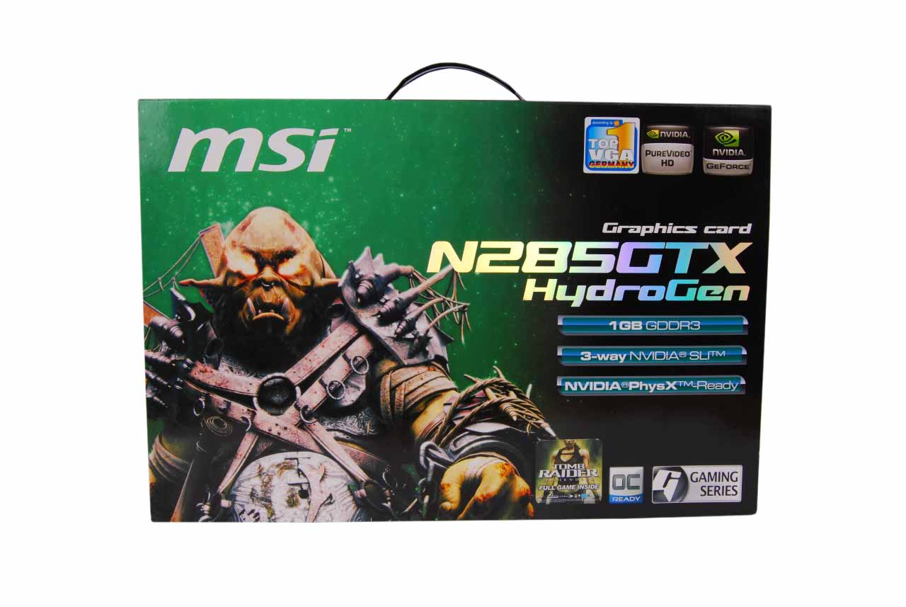
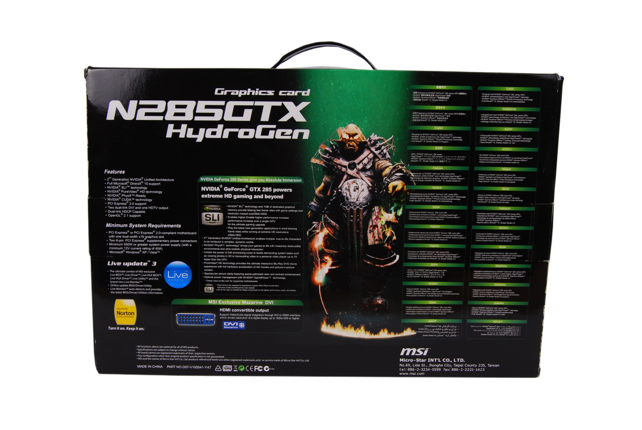
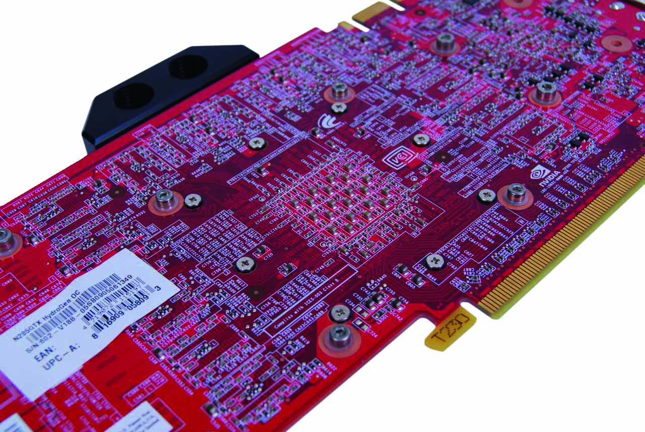
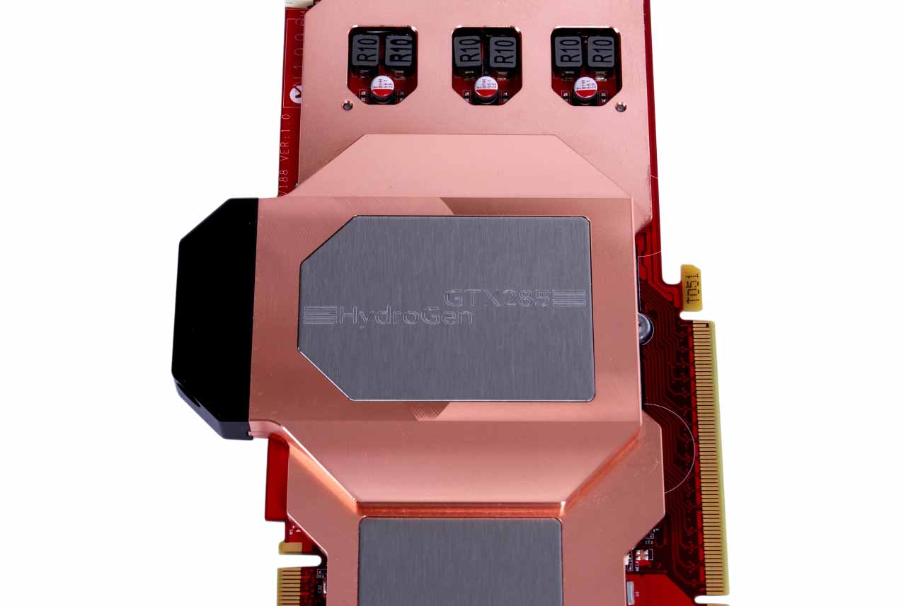
MSI GTX 285 HydroGen OC Review MSI GTX 285 HydroGen OC MSI GTX 285 HydroGen OC Review MSI GTX 285 HydroGen OC
Click to enlarge

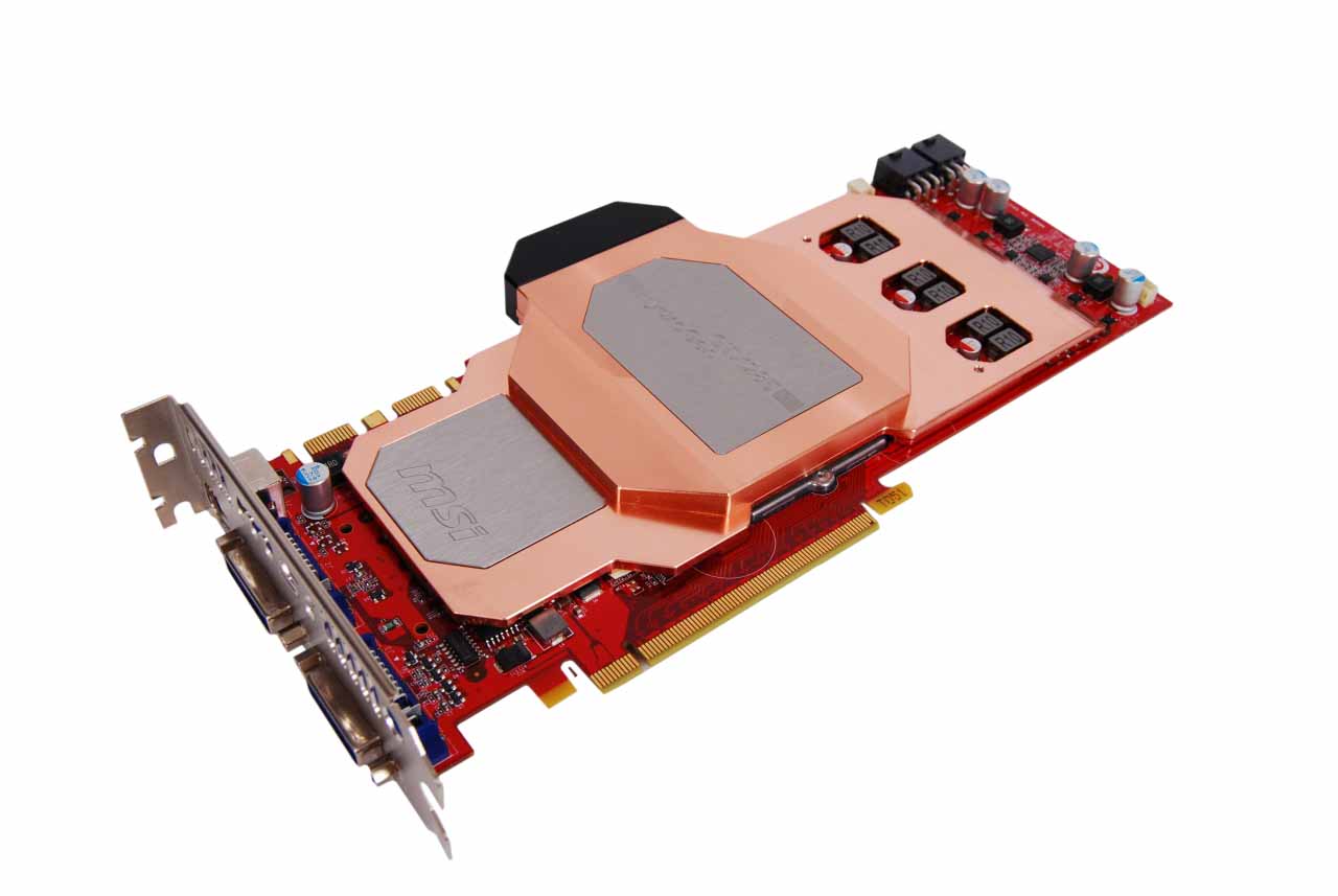
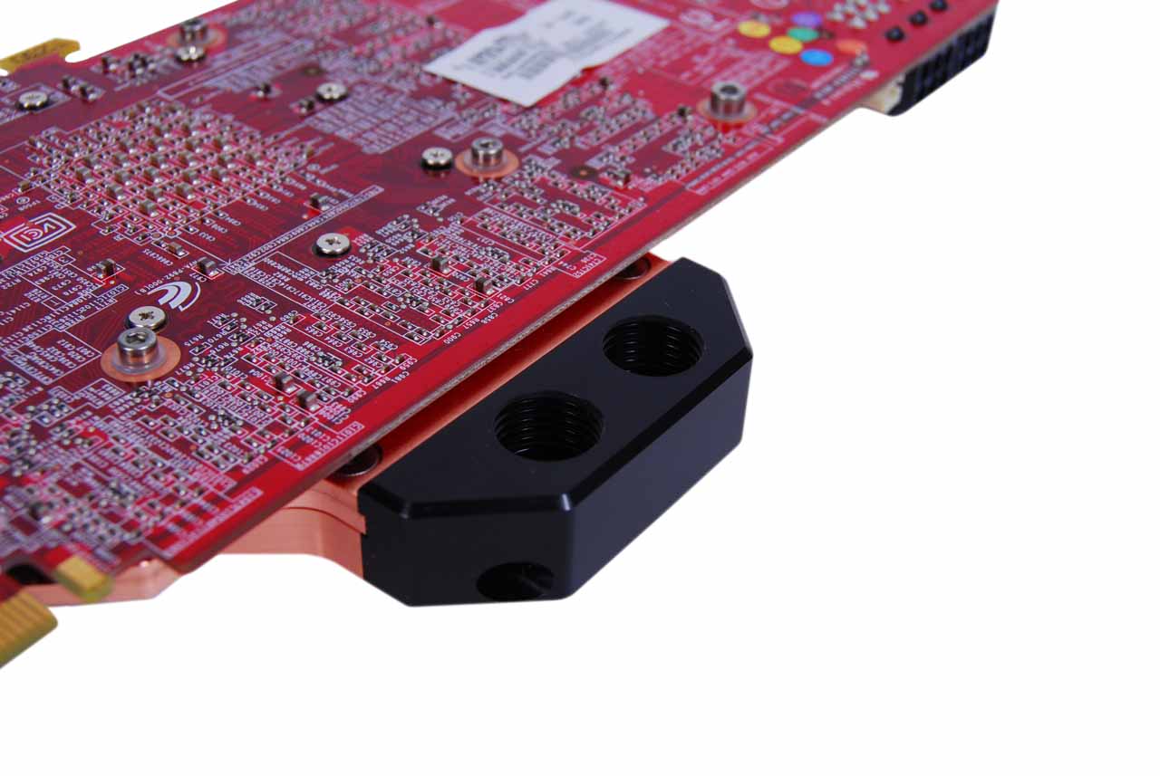
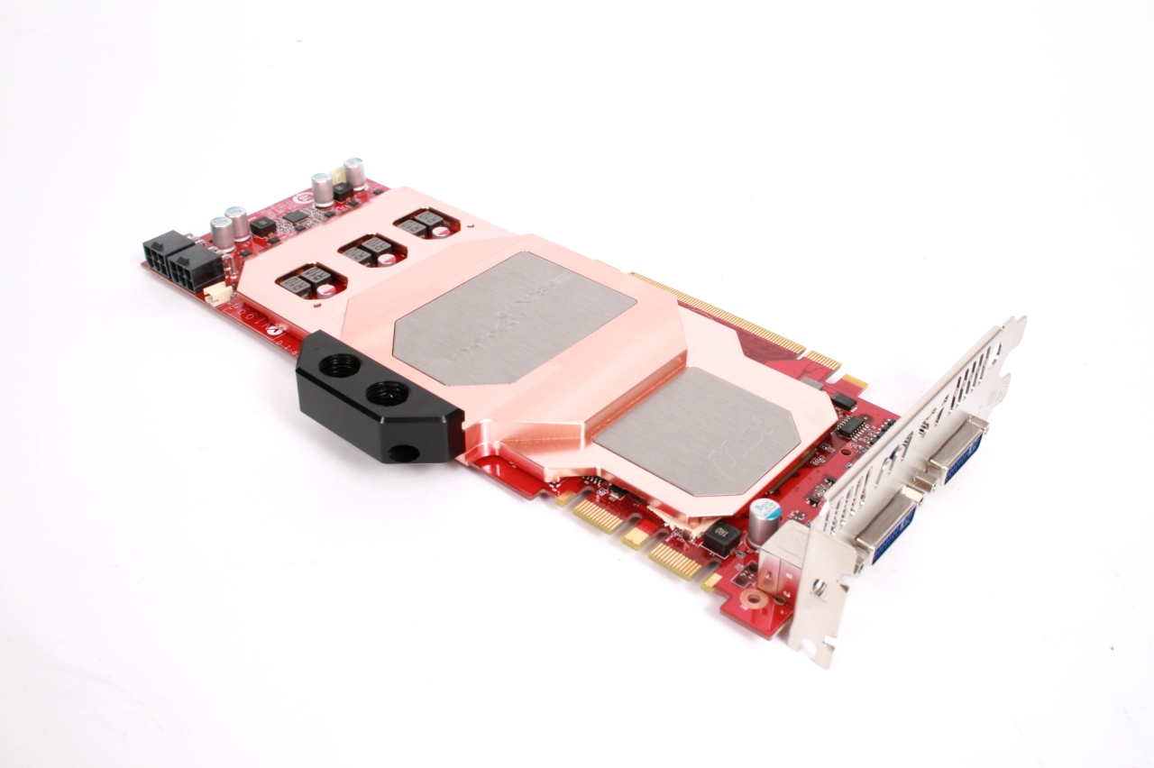
We've come accross the HydroGen range before when we looked at the MSI GeForce GTX 280 OC HydroGen in comparison to a BFG GeForce GTX 280 H₂OC. The former used a Heatkiller full cover waterblock from German manufacturer Watercool, which cooled the core, RAM and VRMs on the core side of the PCB. Our findings were that the Heatkiller block provided great cooling at a cost of flow rate thanks to increased pressure as the internals proved to be quite impinging. You will of course need your own water-cooling kit to bolt it into, but the GTX 285 HydroGen OC can easily be added to an existing loop, whatever size tubing you're using.

MSI GTX 285 HydroGen OC Review MSI GTX 285 HydroGen OC MSI GTX 285 HydroGen OC Review MSI GTX 285 HydroGen OC
Click to enlarge

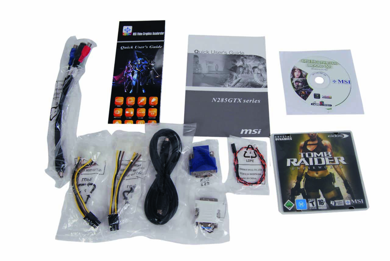
Watercool is back with MSI's latest foray into water-cooling its wares, with the latest Heatkiller GPU-X² full cover block strapped to MSI's GTX 285 HydroGen OC graphics card. It's a similar package to what we saw last time as pictured below, including a DVI to HDMI adapter, two molex to 6-pin PCI-E power connectors and a copy of Tomb Raider: Underworld worthy of note. Unfortunately we had to fish around for our own barbs as the GTX 285 HydroGen OC doesn't include any.

The threads are G1/4" so are compatible with a vast majority of barbs out there, but still, it wouldn't hurt to include some for 1/2"ID tubing seeing as this, and 7/16" ID which also fits, are by far the more popular choices at the moment.

MSI GTX 285 HydroGen OC Review MSI GTX 285 HydroGen OC MSI GTX 285 HydroGen OC Review MSI GTX 285 HydroGen OC
Click to enlarge

The clock speeds have of course been overclocked with the core being boosted from 648MHz to 702MHz and the memory clock from 1,242MHz (2.484GHz effective) to 1,300MHz (2.6GHz effective). The shader clock however hasn't been touched and remains at 1,476MHz which might mean results aren't much improved over a stock GTX 285. The great thing about water-cooling though is that the extra heat generated from overclocking a graphics card is dealt with quickly and quietly with modern water-cooling hardware, such as the Swiftech parts in our test kit.

There's no noisy fan spinning up during games either and it's usually very interesting seeing how much further we can push water-cooled graphics cards, even if they're pre-overclocked. More on that later, but the question as always is how much the MSI GTX 285 HydroGen OC goes to justifying its hefty £389 price tag: that's roughly £100 more than an air cooled pre-overclocked GTX 285!

The Heatkiller GPU-X² water block

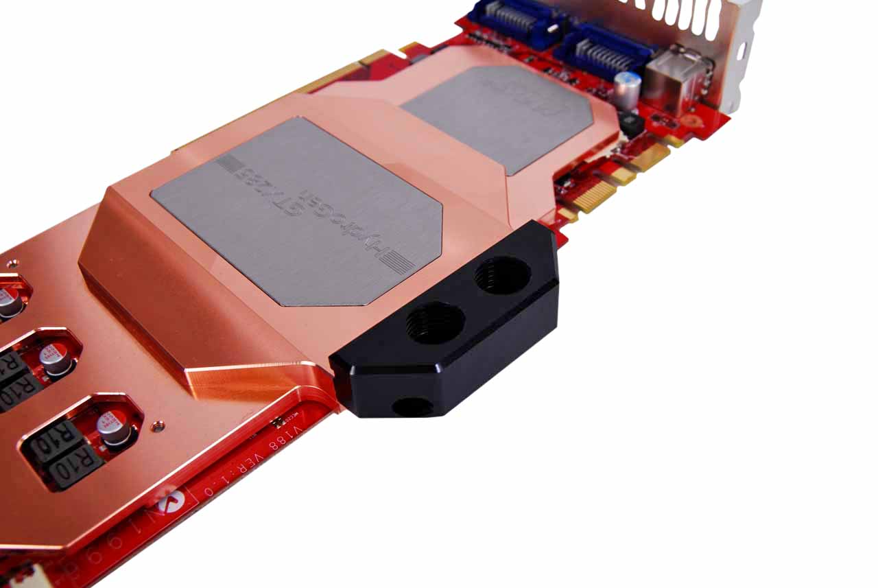
MSI GTX 285 HydroGen OC Review The Heatkiller GPU-X² water block Something that bothered us with the GTX 280 HydroGen OC was the fact both barbs have to face the same way. Unfortunately the same is true of the MSI GTX 285 HydroGen OC. A black acetal port mount is secured to the block by means of two hex screws. This can be removed and inverted so at least your not stuck with having your barbs facing in just one direction (up is default).

Inverting the port mount is relatively easy. The only thing you have to watch is the rubber o-ring that sits between the block and the mount providing a seal. Even so, plumbing in two or more cards like this would quickly prove to be a bit of a nightmare and would look pretty ugly too.

If you're planning an SLI system though, you have two options. Water-cool offer a 4-way adapter for the Heatkiller GPU-X² water block which replaces the stock port mount with one with two ports on the top and bottom with a similar configuration to other water blocks. They also offer adapters than can link two or three blocks.The other option is to opt for a Dangerden or EK full cover waterblock which usually have four ports as standard.

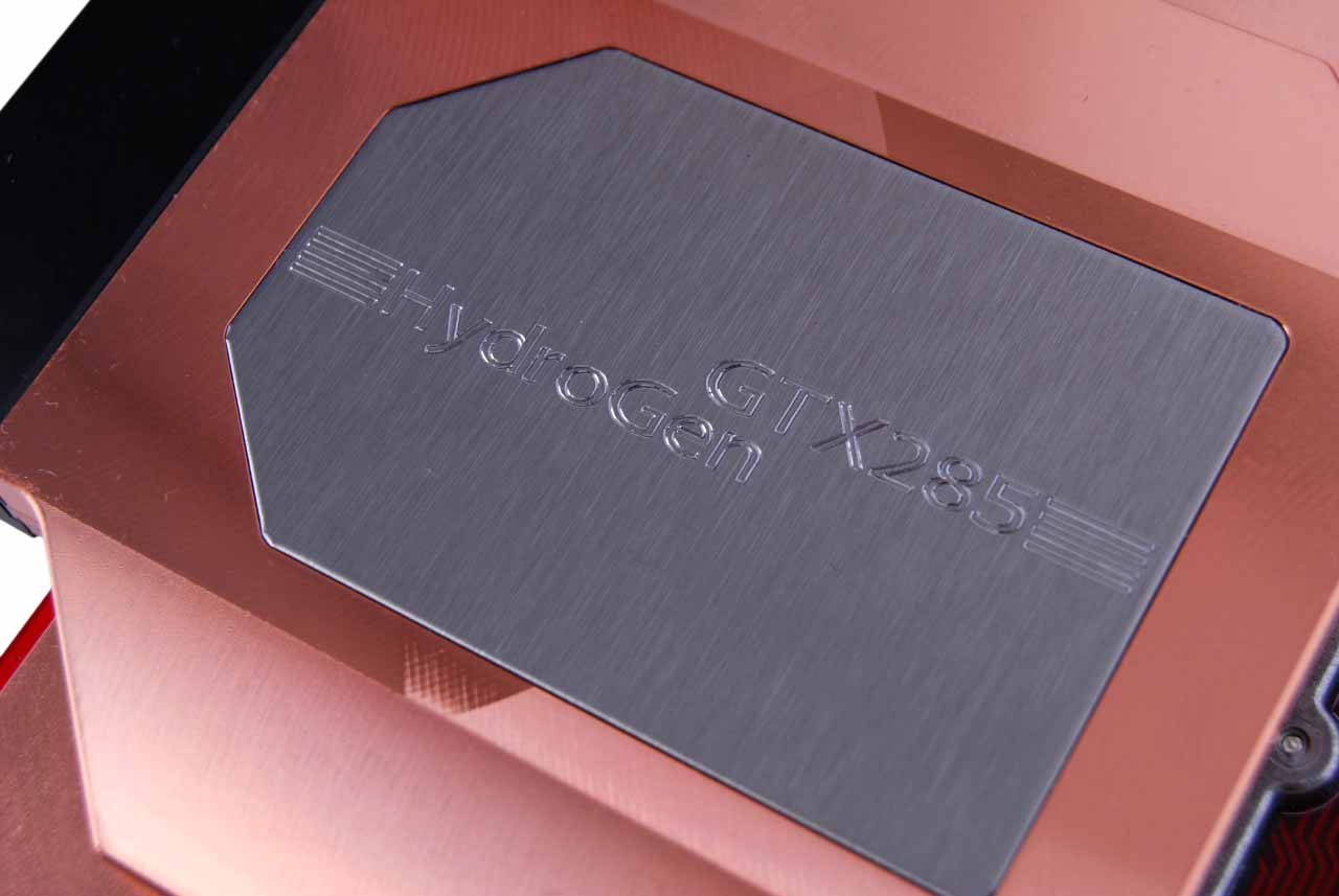
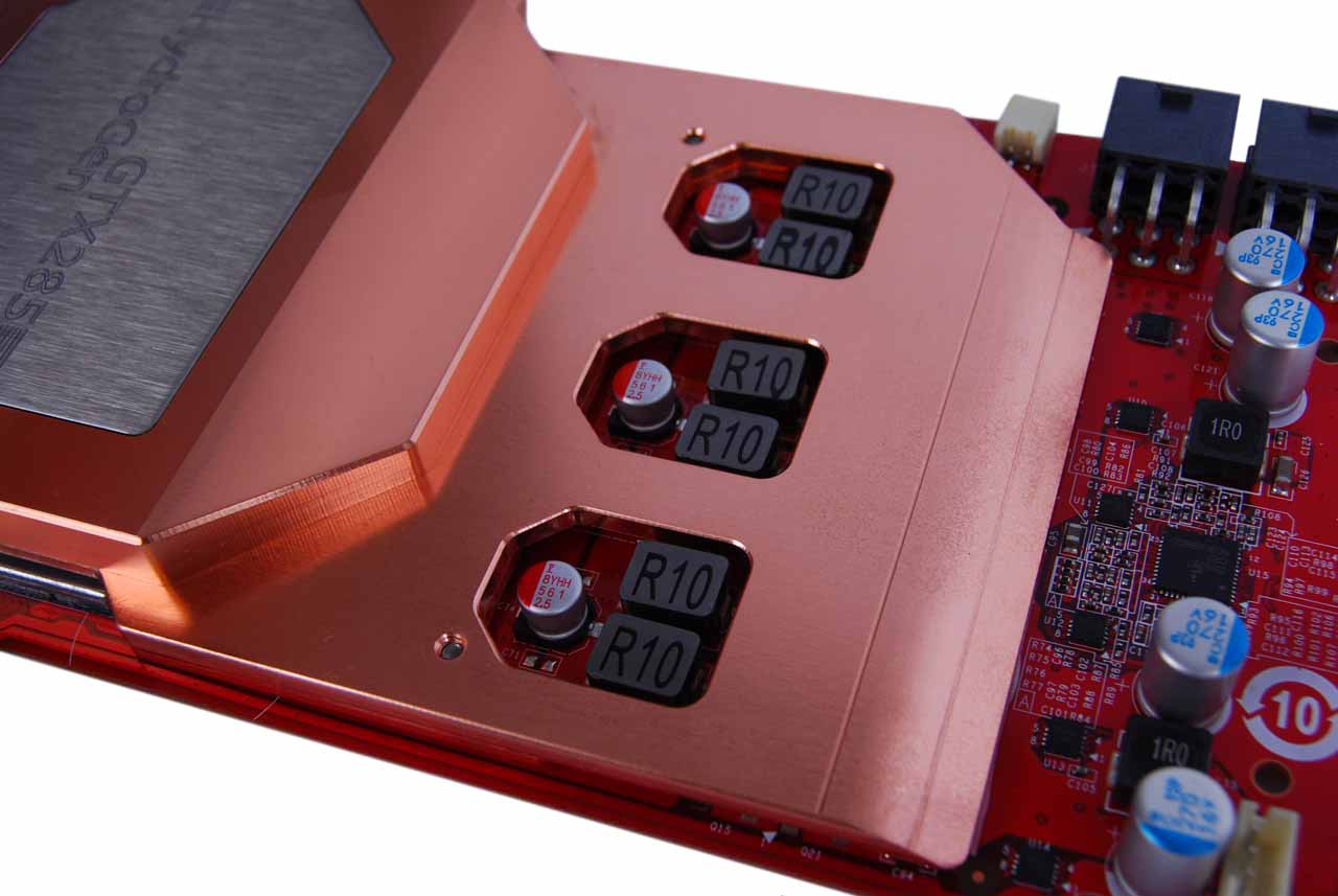
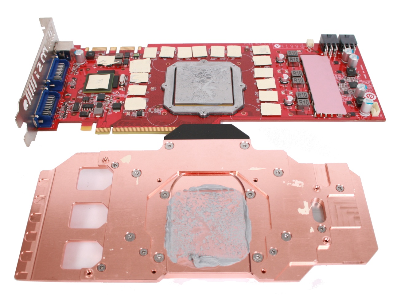
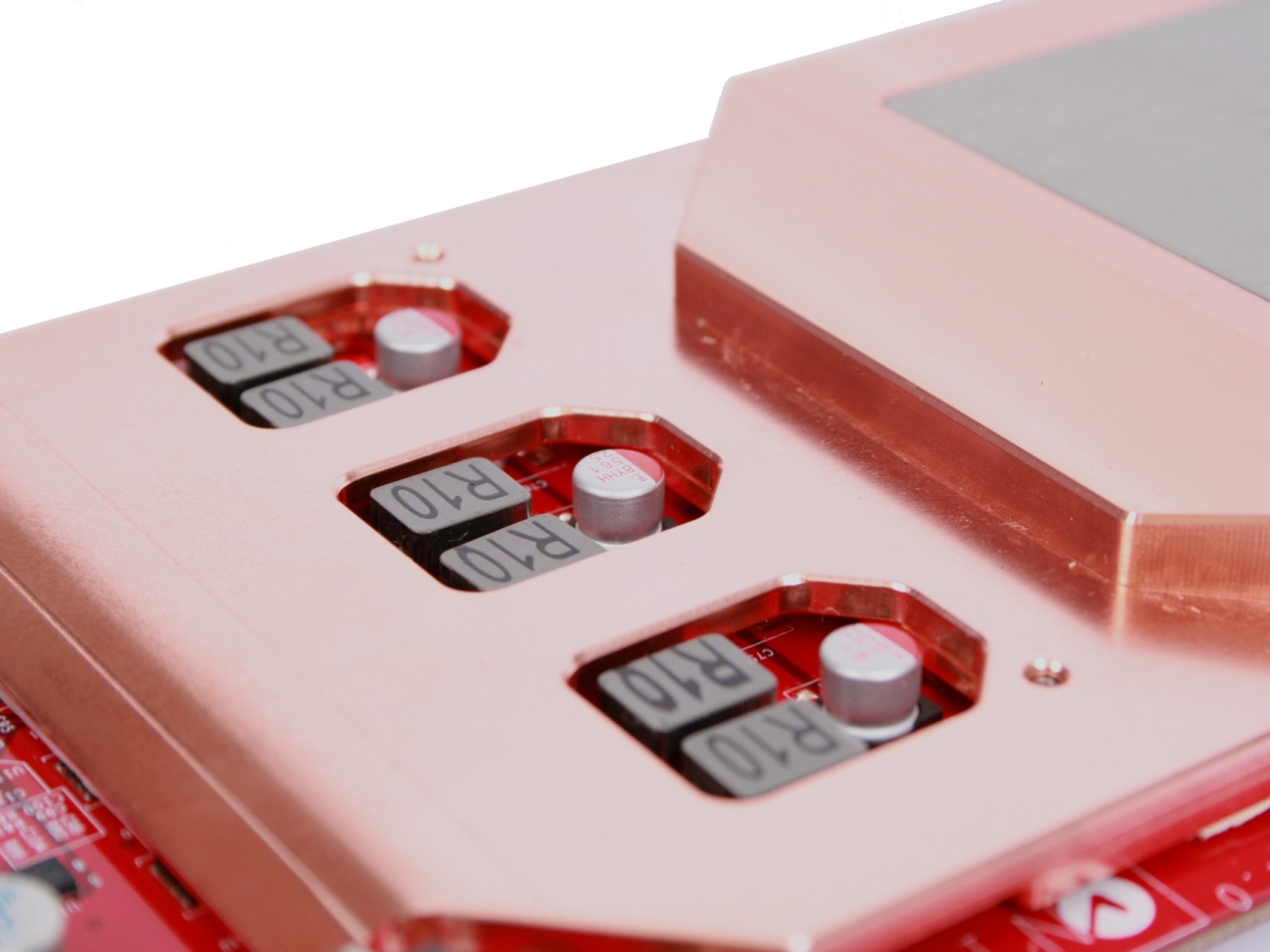
The block itself is a work of art and typical of German engineering. It's slimmer than other blocks we've seen and it hugs the PCB from front to back, neatly slotting itself between capacitors and easing in between other parts of the VRM circuitry, at the end of the PCB (Ed: That was somewhat erotic, Antony!).

There are a total of sixteen mounting screws securing the block to the PCB on the topside, and as all the RAM chips are located on same side of PCB, you don't have to worry about adding extra ramsinks - something that was a good idea when water-cooling the GTX 280 as the RAM can get pretty darn hot when left to its own devices.

MSI GTX 285 HydroGen OC Review The Heatkiller GPU-X² water block MSI GTX 285 HydroGen OC Review The Heatkiller GPU-X² water block
Click to enlarge

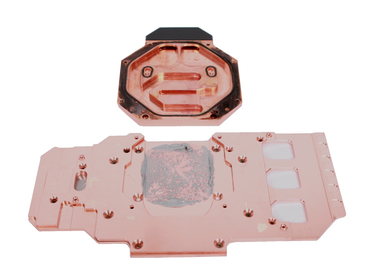
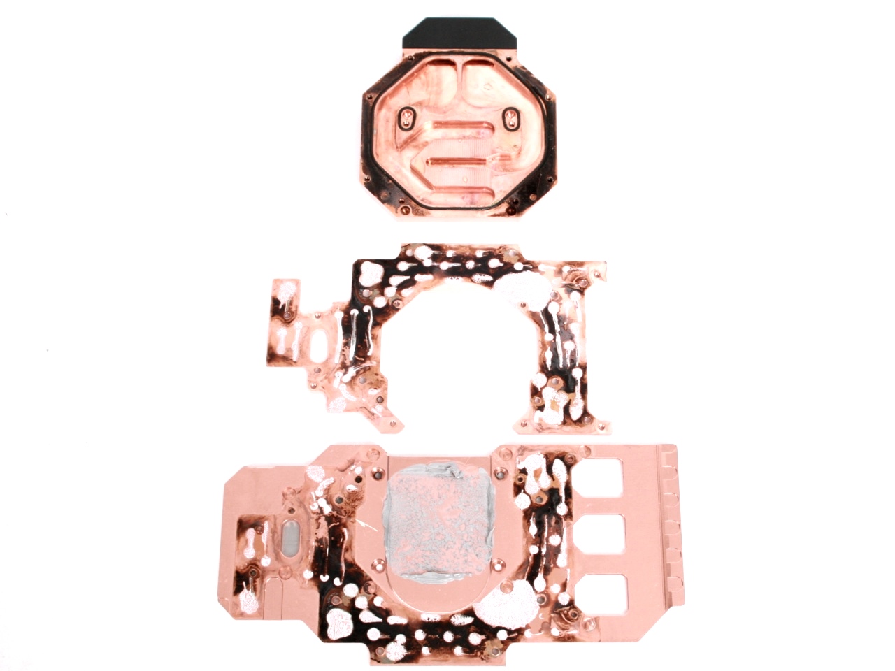
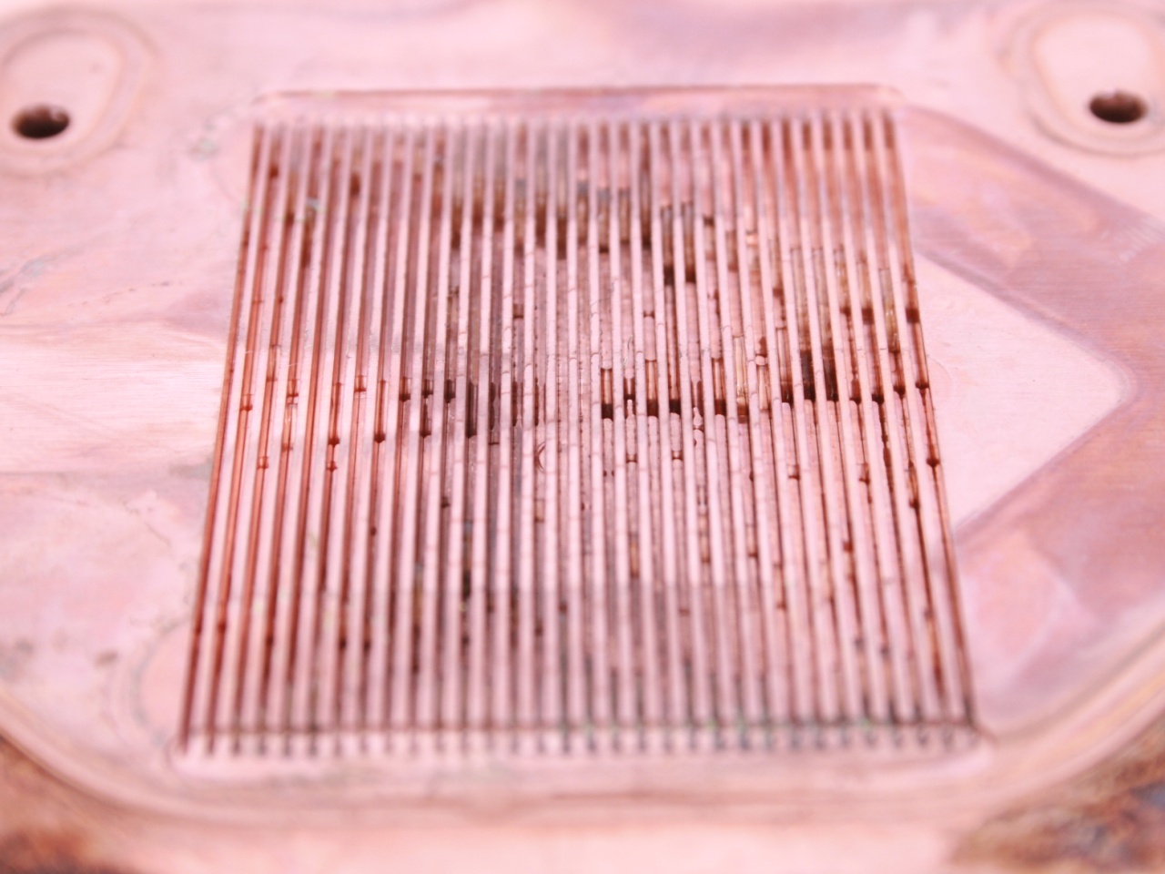
Unlike other blocks we''ve seen, Heatkiller full cover blocks are made up of three main copper parts which fix firmly together. We couldn't help but take a peek inside and what we saw was a very different design to the likes of Dangerden and EK Waterblocks. On the other side of the narrow inlet and outlet are two channels separated by a bridge of copper. On the contact plate are a series of extremely fine channels through which the coolant is forced, each being less than half a millimetre wide.

MSI GTX 285 HydroGen OC Review The Heatkiller GPU-X² water block MSI GTX 285 HydroGen OC Review The Heatkiller GPU-X² water block
Click to enlarge

We haven't seen channels this fine since the XSPC Edge CPU block, and that was discontinued due to the fact that making fins this small is so difficult. We're not quite sure what the black residue is but as it's only located inbetween the copper plates, it's most likely some form of thermal paste.

MSI GTX 285 HydroGen OC Review The Heatkiller GPU-X² water block MSI GTX 285 HydroGen OC Review The Heatkiller GPU-X² water block
Click to enlarge

As we've already mentioned, the Heatkiller has a higher impingement than other blocks we've seen. The inlet and outlet ports in particular are very slim indeed which can only lead to higher pressure inside the block and in theory better performance. This is certainly what we saw when comparing the BFG GeForce GTX 280 H₂OC and the MSI GTX 280 HydroGen OC, with the latter managing noticeably lower temperatures.

The downside to this is that the Heatkiller block isn't as well suited to loops with a significant amount of hardware, with EK and Dangerden blocks offering lower impingement. However with modern powerful pumps such as the Laing D5 or DDC-1T Ultra, the difference will be negligible in most situations.

MSI GTX 285 HydroGen OC Review The Heatkiller GPU-X² water block MSI GTX 285 HydroGen OC Review The Heatkiller GPU-X² water block
Click to enlarge

There's also next to no room between the barbs once you've thrown some 1/2"ID tubing on, so jubilee clips only just fit, but there's a fair it of wriggling required. This also meant that straight 1/2" compression fittings didn't fit either although we found that Feser 45 degree rotary fittings do fit following a little persuasion.

How we tested

As always, we do our best to deliver a clean set of benchmarks, with each test repeated three times and an average of those results is what we’re reporting here. In the rare case where performance was inconsistent, we continued repeating the test until we got three results that were consistent.

The tests performed are a mixture of custom in-game timedemos and manually played sections with FRAPS to record the average and minimum frame rates. We strive to not only record real-world performance you will actually see, but also present the results in a manner that is easy to digest.

Water-cooling setup

To test this card we fashioned a graphics card-only water-cooling loop from components that we had in the Lab. We settled for a single 120mm radiator with a high rpm fan, a small reservoir, a powerful pump and 1/2in inner diameter tubing. Here’s the full setup:
  • Danger Den Black Ice Pro radiator (single 120mm)
  • Laing D5 pump
  • Swiftech MCRES-Micro reservoir
  • 1/2in inner diameter tubing
  • De-ionised water with Swiftech Hydrex additive

*MSI GTX 285 HydroGen OC Review Test Setup *MSI GTX 285 HydroGen OC Review Test Setup
Click to enlarge

Intel Core i7 Test System

Intel Core i7 940 processor (operating at 3,709MHz – 22x168.6MHz); MSI Eclipse SLI motherboard (Intel X58 Express with three PCI-Express 2.0 x16 slots); 3x 2GB Corsair TR3X6G1333C9 memory modules (operating in dual channel at DDR3 1,349.4MHz 9-9-9-24-1T); Seagate Barracuda 7200.11 250GB SATA hard drive; Corsair HX1000W PSU; Windows Vista Home Premium x86-64 (with Service Pack 1); Intel inf 9.1.0.1007 WHQL.

Nvidia graphics cards

  • MSI GTX 285 HydroGen OC – operating at 702MHz/1,476MHz/2,600MHz using Forceware 185.68 WHQL
  • Nvidia GeForce GTX 275 896MB – operating at 633/1,404/2,268MHz using Forceware 185.68 WHQL
  • Nvidia GeForce GTX 285 1GB – operating at 648/1,476/2,484MHz using Forceware 185.68 WHQL

ATI graphics cards

  • Sapphire Radeon HD 4890 1GB Atomic – operating at 1000/4,200MHz using Catalyst 9.4 WHQL
  • AMD ATI Radeon HD 4890 1GB – operating at 850/3,900MHz using Catalyst 9.4 WHQL
  • AMD ATI Radeon HD 4870 X2 2GB – operating at 750/3,600MHz using Catalyst 9.4 WHQL

Games Tested

  • Fallout 3, version 1.4.0.6 with DirectX 9.0
  • Far Cry 2, version 1.02 with DirectX 10/10.1 and DirectX 9.0
  • Crysis, version 1.21 (64-bit) with DirectX 10
  • Call of Duty: World at War, version 1.3.1080 with DirectX 9.0
  • S.T.A.L.K.E.R.: Clear Sky, version 1.5.07 with DirectX 10/10.1
  • Race Driver: GRID, version 1.2 with DirectX 9.0

DDR3-2000+ Memory Kits - Fast but Flawed

We just looked at i7 memory scaling performance and now it is time to chill a few processors to see what those DDR3-2000+ kits are capable of for the serious overclocker. As it turns out that was the opening to our original article, which we planned to launch in conjunction with the DDR3 memory-scaling article.

However, the best plans of mice and men sometimes go awry. Unfortunately, we met delay after delay as every one of our Elpida “Hyper” based kits failed on us in some form or fashion over the past few weeks. At times, a single module would fail and eventually the whole kit in certain instances. Eventually our patience wore thin as even warranty replacements started failing and we knew this was not an isolated problem.

In fact, this problem has become widespread in the extreme overclocking community. Admittedly, widespread in this particular group means a few hundred users. Nevertheless, this audience purchases these extreme memory kits with prices tags reaching the $500+ level at times and expects like performance and quality in return. Certainly, the performance is there, quality we are not so sure about right now.

We could attribute the demise of our modules to the elevated voltage levels we have used for this article and normally we would go that direction and stop for the day. However, we had modules die on us using no more 1.50V VDimm and stock VTT settings in a variety of boards. We are not the only ones, as it seems a number of users have also been through the RMA process (a few more than once) regardless of voltage settings.

The “official” cause of death is unknown at present, while the usual suspects, such as manufacturing errors, motherboard voltage/ user over voltage issues and temperature related deterioration are the obvious perpetrators. The “unofficial” cause of death is simply a quality problem with the Elpida “Hyper” based ICs according to various sources we have spoken with the past couple of weeks. Granted, the other factors can and probably do account for a certain failure rate, but the randomness of our failures along with others, especially at first POST or during stock benchmarking lead us to believe that the quality of the IC is the primary factor at this point.

We have contacted Elpida about the problem but do not have an “official” response from their engineering group yet. However, the problem is serious enough that Corsair informed us earlier today that they asked their retailers to return any kits in the channel. They will not be selling kits based on the Elpida Hyper ICs until an enhanced manufacturing and testing process is in place to ensure the quality of this particular product before shipment. We applaud Corsair for being aggressive in regards to this problem and we expect/hope other suppliers to follow suit.

Most of the suppliers have reported that a relatively small percentage of kits appear to be affected. Just how small is unknown. Based on our own numbers and those of other users it appears to us it is significantly more serious than we were lead to believe a few weeks ago. We are now at the point of just saying that you are better off avoiding Elpida Hyper kits due to the ‘frequently random’ level of failures with modules. However, at least for now, all of the suppliers are fully backing their warranties. If you need the available benchmarking performance generated by these kits then it is worth the risk. Just make sure of the warranty terms before purchase, or simply put, buyer beware.

When we speak of failures, there are two types, a catastrophic failure where the module dies instantly and one of deterioration. One or more of the modules failing to map fully to the operating system usually marks the first sign of deterioration. Moving the modules around between the slots can work around some of this, although from our experience this is a primary sign that things are beginning to go downhill fast. This phenomenon is not to be confused with the i7 memory controller skipping to map a module because of insufficient voltages for the applied clocks.

The next step is when the module no longer clocks up at stock voltages or given voltage limits like 1.65V VDimm. We have witnessed modules not clocking above 1900MHz or so regardless of voltages and slowly dropping to 1200MHz before total failure.

With all that said, we decided to complete the article as there are users out there that have not experienced any of the issues at all or those still wishing to take a chance on these kits. Two of the kits we have been pushing for raw bandwidth over the past few weeks are Corsair’s Dominator GT 7-8-7-20 6GB kit and OCZ’s Blade 2133 8-9-8-24 6GB kit. We have tested other kits, but these are the last two standing in the labs although both of them are now showing signs of deterioration.

Corsair chose to stick with the tried and tested 2000MHz CAS 7-8-7-20 formula while OCZ gives up the tighter CAS rating in a bid to woo the market with a 2133MHz kit at 8-9-8-24 timings. On the face of it, we would say that both kits should be capable of similar results assuming that SPD and PCB differences between the two are not massive. OCZ and Corsair tell us their respective top end kits represent the top 1% of the Elpida Hyper yield.

We’re keeping it simple today, running a few of the preferred benchmarking programs in a bid to find maximum frequency limits for the modules along with a small comparison of scores at the same CPU frequency. We have already shown that these kits are not really needed by the general enthusiast and typically do not improve application performance significantly enough to warrant the increased cost. However, they do provide a certain degree of flexibility when overclocking and allow for very tight latencies at a variety of memory speeds.

Test Bed Setup

Windows XP is still the preferred operating system for 90% of the synthetic and 3D programs when benchmarking. We also utilized Vista 64 Ultimate to confirm memory stability in some of the 3D benchmarks with the entire memory footprint mapped and available. This allows us to find bandwidth limits at heavier system loads than those imposed by Super Pi under XP Pro.

We ran each benchmark five times with the high and low scores tossed out and the remaining scores averaged. We utilized fresh operating system installations for each memory kit. We reboot the system between each benchmark program change, clear the prefetch folder, and then defragment the drive between reboots to ensure the results are consistent.

We’ve got a choice of 3 sub-zero temperature friendly CPU’s in the labs (all D0 stepping). Surprisingly enough the 975 D0 taps out earliest, and just about crawls to 5GHz providing the QPI link frequency multiplier is left at the lowest possible setting. We had expected this processor to give us the requisite flexibility of pushing these kits to the pinnacle of their ability, but the i7 920 and W3540 Xeon proved to be the better choice for raw bandwidth on both sides of the bus.

We matched memory sub timings on both modules, right down to Round Trip latency parameters in a bid to ensure that maximum frequency scaling is not hindered by incorrectly sensed values. EVGA’s Classified E760 motherboard provides BIOS level overrides for almost all memory parameters as well as auto presets for all available sub-timings based on SPD information.

CAS Fashion Question: Is CAS 8 the new CAS 7?

We’ll start off with Super Pi to check frequency scaling. We set a memory voltage ceiling of 1.85V, which we think is more than most users will ever push into their Hyper based modules for benching. For 24/7 use, we do not suggest more than 1.72V based on conversations with the memory suppliers, actually less is more in this case.

The Corsair modules offer just slightly better voltage/frequency scaling in the Super Pi results. We attribute most of the differences here to the variances in the kits we received. The original Corsair kit actually generated slightly lower results when it came to maximum memory clocks. Our first Blade kit was marginally better when it came to voltages at like settings. The kits tie where the CPU is the limiting factor once we are over 2300MHz with CAS 8-9-8 timings.

Peak gains when using a higher memory bandwidth are certainly apparent between CAS 6 and CAS 7. With the Uncore multiplier at 16X, CAS 6 on the 2:8 memory ratio loses around 10 seconds to CAS 7 running at 2094 MHz with an Uncore multiplier of 20X. In case you’re wondering why there are no Corsair results at CAS 7-7-7 timings, it because out of the six modules we have in the labs, none will post consistently over 1950MHz with CAS 7-7-7 timings at this point. This is irrespective of VDimm settings or swapping the modules around in the slots as we notice early deterioration setting in at this point. In fact, a couple of the modules are already near a 1500MHz limit.

Oddly enough 7-8-7 or 8-9-8 timings still work fine on several of the Corsair modules at 2000, provided we put the module into the right slot to initialize the POST process. This simply comes back to the modules deteriorating through the course of our testing. Our OCZ Blade modules can be plugged in at these timings and still POST although we have started to encounter a few module swap requirements. We are not ruling the board or voltages completely out of the equation just yet, but based upon previous testing results we do not believe the situation is specific to either variance as one of our OCZ modules already failed at stock voltages.

Even a matched Uncore multiplier at CAS 6 is not sufficient to eclipse the CAS 7 2094 MHz 32m time. The Everest results for these 2 test points do confirm the performance advantage of having higher bandwidth and 2ns faster access latency.

Perhaps more interesting than the raw gain versus memory frequency is something we found out during our tests of the EVGA Classified a couple of months ago. The light capacitive load of the Hyper modules allows higher overall processor clocks than memory kits based on Micron or Samsung based parts, reliability issues withstanding of course.

CAS 7 is likely to be the preferred latency setting for most benchmarks, providing enough flexibility for scaling processor clocks right to the limits of the silicon, especially when using locked multiplier CPU’s. Running either set of modules at CAS 8 to around 2250MHz does allow the use of slightly more conservative memory voltage at the cost of the low acess latency of CAS 7-7 timings around 2100MHz. We added a couple of maximum frequency runs above just to show how it all adds up.


A few 3D results...

Let’s take a quick look as to how 3D benchmarks such as 3DMark Vantage, 3D Mark 06 and 3D Mark 05 are believed to be somewhat affected by memory bandwidth. Vista 64 allows us to see how the memory voltages we utilized for Super Pi apply to a 64 bit OS when all 6GB of memory is fully mapped.

No major gains here in 3DMark Vantage as we have a 100-point difference between CAS6 1836MHz and CAS8 2294MHz.. Voltage wise, we see the need for an elevated idle voltage in Vista due to increased voltage droop under load with 6GB fully mapped. The actual load Vdimm in these benchmarks is exactly the same as what we used for Super Pi 32m under the XP operating system.

3D Mark 06 scores more consistently run to run than Vantage and seems to prefer the tighter CAS latency of 6, giving a 400 point boost.

Switching over to XP for 3D Mark 05 we find that the GPU benches are not overly sensitive to CAS or memory bandwidth. The best overall scores come when using the 20X Uncore multiplier on our 920 CPU (one below the CPU core multiplier). Using higher Uncore multipliers than the CPU core multiplier actually resulted in lower average results for 3D Mark 05, due to the additional hold times asserted by the IMC to the clock crossing process. This performance offset can be seen in BIOS via the increased Round Trip Latency values. In essence you get faster L3 cache performance while the IMC slows down memory bus transfer times to levy the increased performance on the other side of the bus; giving up one for the other. Bottom line here is that higher Uncore frequencies don't really offer anything exciting in any benchmark that reads or writes more data than the CPU cache can hold. As an example running a 23X Uncore multiplier results in a 15ns shift for the worse in Round Trip Latency which cannot be reclaimed with the current range of settings availble withn the EVGA BIOS. Higher Uncore frequencies may appear attractive at first approximation, but they're not always best in every scenario.

Using CAS 6 also resulted in the GPU tests of 3D Mark 05 failing to pass at 229 BCLK regardless of voltages, while running 2294 MHZ CAS 8 with the same Uncore multiplier passed without a glitch.

Final words

We had certainly hoped to provide a review with all of the latest DDR3-2000 6GB kits, but it was just not meant to be considering the failures encountered during testing. Based upon the frequencies and timings of the Elpida Hyper based modules from OCZ and Corsair, these kits offer nearly the same performance with voltage requirements favoring Corsair although this can be attributed to the variances in the kits we received.

We would love to recommend either one to any user who is fanatical about benchmarking or just having the best product in their system. Unfortunately, it is not something we can do based upon the current reliability issues. We accept that elevated voltage levels above 1.65V are out of potential warranty levels, even though Elpida designed the IC to scale with voltages up to 1.85V. However, the deterioration/failure of this particular IC seems to be far in excess of anything we have had in the labs for quite a while.

Based on our own experience the failures are not vendor specific as modules from all the major suppliers have died on us. We lost modules using as little as 1.50 VDimm, on five different Intel boards, an AMD AM3 board, and at various temperatures on the modules and IOH. These failures are not solely confined to a particular slot location, parts combination, or BIOS design, leaving little doubt that there is a quality assurance problem at Elplida. Whether that quality problem is based on a lack of proper screening, process controls, engineering design, or a combination of all three is something we may never know.

What we do know is that Corsair, OCZ, and others are honoring their warranties with Corsair now reaching the point of pulling their kits from the retail channel until these problems with Elpida are addressed. Whether other suppliers follow suit or not is something we are trying to verify at this point, although initial conversations indicate this might happen.

If you are shooting for world records, then there really is no other choice at present, it’s pretty much Elpida Hyper or bust when you look at top scores on the i7 platform on the Orb or HWbot. Of course, that does not matter if the kits fail on you during a benchmark run or are unavailable. We hear rumors that Samsung might have something in the pipeline shortly that will at least mimic the high bandwidth of the Elpida Hyper at low voltages. We hope that performance will come without the attendant reliability problems we are suffering with currently.

There is a glimmer of hope as a select few users seem to have a bit of luck and have had no failures at all, even after months of usage. The question is at $500 a pop for these particular kits, do you feel lucky enough to take the risk?